High Resolution Conductive silicon probes
Brand:
Category:
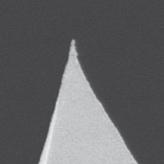
DPER probes are made by depositing a thin platinum coating on silicon tips. While the thickness of the coating on a flat cantilever surface is about 15 nm, there is only a 10 nm increase in the tip dimensions compared to bare silicon probes. These probes are recommended for electrical applications requiring higher resolution.
Pt coated resulting tip radius .............................. < 20 nm
Pt overall coating ..............................15 nm
Technical Features
| Cantilever Series | Length l, ± 5 μm | Width w, ± 3 μm | Thickness ± 0.5 μm | Res. Freq. kHz Typical | Freq. Rison. kHz Range | Const. Force N/m Typical | Const. Force N/m Range |
|---|---|---|---|---|---|---|---|
| HQ:DPER-XSC11 | |||||||
| HQ:DPER-XSC11 lever A | 500 | 30 | 2.7 | 15 | 12 - 18 | 0.2 | 0.1 - 0.4 |
| HQ:DPER-XSC11 lever B | 210 | 30 | 2.7 | 80 | 60 - 100 | 2.7 | 1.1 - 5.6 |
| HQ:DPER-XSC11 lever C | 150 | 30 | 2.7 | 155 | 115 - 200 | 7 | 3 - 16 |
| HQ:DPER-XSC11 lever D | 100 | 50 | 2.7 | 350 | 250 - 465 | 42 | 17 - 90 |