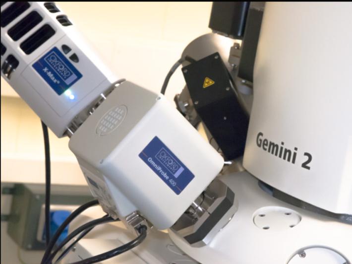
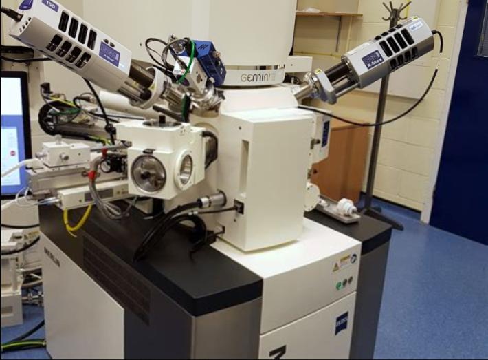
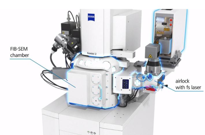
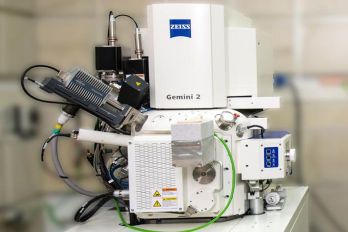
The FIB-SEM from Oxford Instruments is a highly advanced tool that combines the capabilities of a Focused Ion Beam (FIB) and a Scanning Electron Microscope (SEM) to provide detailed characterization of samples at the nanometric level. This versatile system is designed for applications requiring high-precision analysis, such as nanotechnology, materials science, semiconductor research, and many other fields.
The FIB enables extremely precise milling of samples, creating thin cross-sections for SEM analysis and allowing for nanometric-level micro-manipulation. Its high resolution and ability to work on very small samples make it essential for sample preparation for advanced studies.
The SEM, on the other hand, is used to obtain high-resolution images of the sample surface, enabling the analysis of morphology, composition, and structural characteristics. The ability to combine BSE (Backscattered Electron) imaging with EDX (Energy Dispersive X-ray Spectroscopy) significantly enhances the system’s versatility, allowing for the precise exploration of both the morphology and chemical composition of the sample.
One of the distinctive features of this system is its ability to perform 3D tomography, using FIB scanning to obtain thin slices that are then reconstructed into a three-dimensional map. This allows for a detailed analysis of the internal structures of samples.
The system is equipped with advanced software that enables real-time data processing, high-precision visualization, and the generation of quantitative reports for a deeper understanding of the results. The FIB-SEM is ideal for a wide range of applications, including the characterization of nanomaterials, semiconductors, advanced materials, and biological samples. Additionally, its ability to perform analyses without permanently altering samples makes it perfect for examining delicate or high-value materials.
In summary, the Oxford Instruments FIB-SEM offers a powerful and flexible solution for nanometric analysis, combining sample milling and manipulation with advanced imaging and spectroscopy in a highly precise and versatile system.
Technical Features
System Overview
The Oxford Instruments FIB-SEM system integrates two complementary technologies:
- The Scanning Electron Microscope (SEM) provides high-resolution imaging of the sample's morphology and chemical composition.
- The Focused Ion Beam (FIB) allows for sample modification through milling, sectioning, and material deposition at the nanometric level.
This combination makes the system ideal for characterization, structural analysis, TEM sample preparation, and nanotechnology applications.
Key Features
Scanning Electron Microscope (SEM)
- Electronic resolution: Up to 1 nm at low beam energies
- Imaging modes:
- Secondary Electrons (SE) for topographical details
- Backscattered Electrons (BSE) for compositional contrast
- STEM mode for transmission analysis
- Beam acceleration voltage: 0.2 - 30 kV
- Detectors:
- SE (Everhart-Thornley)
- BSE (for Z-contrast imaging)
- STEM (for transmission mode)
Focused Ion Beam (FIB)
- Source type: Plasma or Ga+ (Gallium)
- Beam energy range: 0.5 – 30 kV
- Beam current: Up to 100 nA
- Operating modes:
- Sectioning and micromachining (TEM lamella preparation, controlled milling)
- Material deposition (GIS - Gas Injection System)
- Direct ion beam lithography
- Surface modification and nanofabrication
Energy Dispersive X-ray Spectroscopy (EDX)
- Real-time chemical analysis
- High-resolution elemental mapping
- Elemental sensitivity: From Be (Z=4) and above
- Advanced quantitative analysis software
3D Tomography and Volumetric Analysis
- Three-dimensional reconstruction through sequential FIB sectioning
- Software for segmentation and volumetric analysis
Operating Environment & Vacuum System
- Ultra-high vacuum (UHV) system for clean imaging
- Operating pressure: 10⁻⁶ – 10⁻⁷ Torr
- Bakeability: Up to 250°C to minimize contamination
Compatibility & Interface
- Compatible with both conductive and non-conductive samples
- XYZR sample stage movement for nanometric precision
- User-friendly software interface for automated analysis
- Data export in multiple formats compatible with external software
Main Applications
- Nanofabrication & Nanotechnology: Creation of nanostructures via direct ion beam lithography.
- TEM Sample Preparation: Precise thin-sectioning for transmission electron microscopy.
- Advanced Materials Analysis: Combination of SEM imaging and EDX chemical analysis for studying semiconductors, polymers, metals, and ceramics.
- 3D Tomography: Volumetric material analysis with digital reconstruction.
- Materials Science & Failure Analysis: Investigation of material defects and industrial failures.
System Advantages
- Nanometric resolution combining FIB and SEM technologies
- Dual imaging & micro-machining capabilities
- Advanced 2D & 3D analysis software
- Highly flexible for research and industry applications