Backscattered Electron and X-ray ​(BEX)

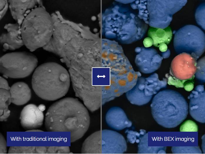
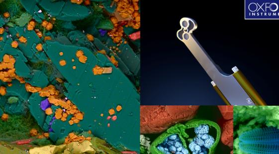
The Backscattered Electron and X-ray (BEX) system from Oxford NanoAnalysis is an advanced tool that combines morphological and chemical analysis of samples on a nanometric scale. It uses backscattered electrons (BSE) to obtain high-resolution images of the material's surface, providing topographical and morphological details. Additionally, it integrates energy dispersive X-ray spectroscopy (EDX), allowing for precise chemical composition analysis, mapping the elements present with high sensitivity, even at low concentrations.

The system is designed to be compatible with SEM and TEM electron microscopes, offering great versatility for applications. With a highly sensitive BSE detector and an EDX detector that analyzes X-rays emitted from the sample, the system provides a comprehensive view of both the physical and chemical characteristics of the sample.

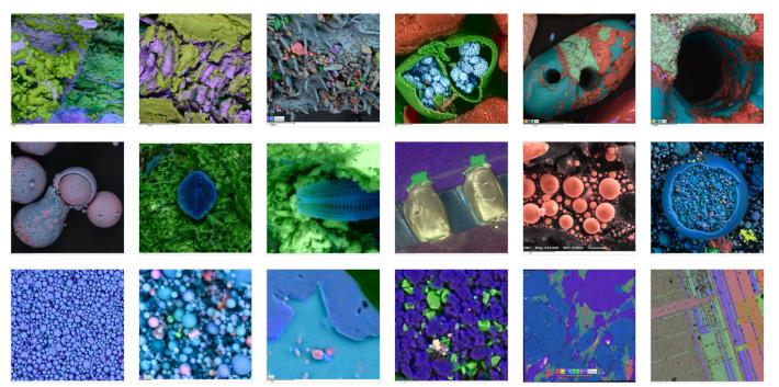
Moreover, the included software enables advanced data visualization and processing, ensuring precise analysis and efficient management of results. The system is ideal for applications in battery materials, nanotechnology, minerals, semiconductors, and forensic analysis, such as gunshot residue analysis.

Technical Features

System Overview:

The Backscattered Electron and X-ray (BEX) system combines high-resolution analysis using backscattered electrons (BSE) with energy dispersive X-ray spectroscopy (EDX), providing comprehensive analysis of surface and chemical composition of samples. Designed for nanometer-scale investigations, it delivers both morphological and chemical characterization of materials with exceptional precision.

Main Features:

  • Backscattered Electron (BSE) Imaging:

    • High-resolution surface imaging for topographical and morphological mapping.
    • Provides contrast based on atomic number differences and surface structure.
    • Ideal for analyzing metals, semiconductors, polymers, and minerals.
  • Energy Dispersive X-ray (EDX) Spectroscopy:

    • Elemental analysis with high spatial resolution and sensitivity.
    • Detects elements at low concentrations.
    • Capable of producing elemental maps to analyze spatial distribution of elements.
  • Detection Systems:

    • BSE Detector: Detects backscattered electrons for surface imaging and characterization.
    • EDX Detector: Analyzes X-rays emitted by the sample for compositional analysis.
  • SEM and TEM Compatibility:

    • Seamless integration with Scanning Electron Microscopes (SEM) and Transmission Electron Microscopes (TEM).
    • Enhances system versatility for various applications.
  • Data Processing and Software:

    • Real-time data visualization and processing.
    • Advanced software for quantitative and qualitative analysis of BSE and EDX data.
    • Supports elemental maps and quantitative spectroscopic data.

Technical Specifications:

  • Energy Range (EDX): 0-40 keV (depending on detector configuration).

  • Spatial Resolution (BSE): Nanometer scale for high-resolution surface imaging.

  • EDX Resolution: Up to 128x128 pixels for elemental mapping.

  • Sample Requirements:

    • Suitable for a wide range of materials: metals, semiconductors, polymers, ceramics, minerals, and biological samples.
    • Compatible with samples of various shapes and sizes, for both SEM and TEM configurations.
  • Vacuum System:

    • Integrated vacuum system for high-performance operation.
    • Optimized for ultra-high vacuum conditions typical in electron microscopy.
  • Software:

    • Intuitive interface for real-time data visualization.
    • Automatic and manual peak identification for EDX.
    • Customizable analysis protocols and data export options.

Applications:

  • Battery Materials: Microstructure and compositional analysis of materials for energy storage technologies.
  • Nanotechnology: High spatial and chemical resolution characterization of nanomaterials.
  • Mineralogy and Geology: Elemental analysis and imaging of minerals for geological studies.
  • Semiconductor Research: Detailed analysis of semiconductor materials for defects, composition, and crystal structure.
  • Forensic Analysis: Detection of gunshot residues, trace elements, and other forensic samples with high sensitivity.
  • Materials Science: Study of surface properties, crystallography, and material behavior in controlled environments.

Advantages:

  • High Sensitivity: Provides reliable results even for trace elements in complex materials.
  • Versatility: Ideal for academic and industrial research in materials science, nanotechnology, and forensic analysis.
  • Ease of Use: Intuitive software with advanced tools for fast and efficient data analysis.
  • Non-Destructive: Suitable for analysis of delicate and valuable samples without altering their properties.

System Configuration:

  • Main Unit: BEX system integrated with SEM/TEM platforms.
  • Detection Unit: High-sensitivity BSE and EDX detectors.
  • Software Suite: Comprehensive software for data analysis, visualization, and report generation.

Optional Accessories:

  • Sample Preparation Tools: For sample preparation and mounting for high-resolution imaging.
  • Specialized Vacuum Systems: For ultra-high vacuum environments to maintain data integrity.

Application Summary:

The BEX system is a versatile tool for high-precision surface and elemental analysis, ideal for materials research, battery technologies, nanomaterial analysis, forensic studies, and semiconductor characterization. It is designed for use in advanced research laboratories, production environments, and industrial applications where detailed material characterization is required.